This post is a continuation of Emulating a GameBoy Cartridge with an STM32F4. Part 1
We have analyzed the memory bus of the GameBoy in order to obtain the timing information of the different signals involved in the read and write operations happening on the cartridge. We will now proceed to develop a system to emulate the behaviour of the cartridge with the STM32F4.
About voltage levels
As we noticed in the previous post, the GameBoy works at 5V whereas the STM32F4 works at 3.3V. We saw that most of the GPIOs of the STM32F4 are 5V tolerant, but they still output 3.3V, so we need to make sure that the GameBoy will detect the high levels properly. Luckily for us, the GameBoy works at TTL level: source. This means that a 3.3V signal will be read as a logic 1 by the GameBoy.
Setup
We will use a similar setup here, although now we are going to connect all the cartridge pins to the STM32F4 so that we can read/write the signals. We have plenty of GPIOs on the STM32F4-Discovery, we just need to make sure we use the 5V compatible ones. I used the following setup:
- CLK -> PC0
- RD -> PC1
- WR -> PC2
- DATA{0..7} -> PE{8..15}
- ADDR{0..15} -> PD{0..15}
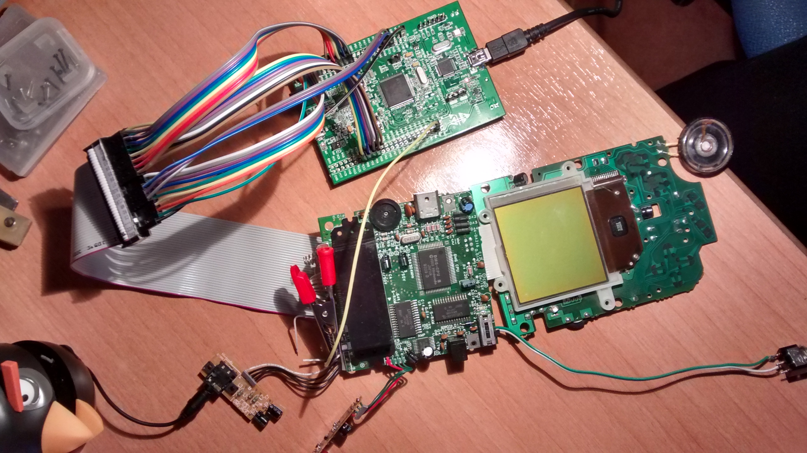
My setup with the GameBoy connected to the STM32F4-Discovery
Coding
The code of this project can be found in my github page under an open source license: github.com/Dhole
Initialization
The initialization code can be found in main.c
The first thing to do is to configure the GPIOs of the board. All the GPIOs are configured as input, push pull mode (will be used when we set the DATA GPIO pins to output) with pull down resistor (I believe pull down resistor is a good choice to avoid current drain from the GameBoy(5V) to the STM32F4(3.3V)). The bus for the GPIOs is configured at 100MHz (maximum frequency available).
This functions can be found in main.c:
void config_gpio_data();
void config_gpio_addr();
void config_gpio_sig();
Secondly, we will configure the CLK to act as a trigger on rise. To do this we enable an interrupt for the GPIO we connected the CLK to that will execute a handler for every level rise. In main.c:
void config_PC0_int(void);Read/Write handler
The read/write handler can be found in stm32f4xx_it.c
The interrupt handler will be executed every time the CLK level goes high (rise). It’s important to notice that there is some delay between the rise of CLK and the execution of the handler. This may be because the GPIOs are peripherials that communicate with the CPU through a bus clocked at 100MHz and also because the interrupt is generated from a peripherial, and thus takes some time to be processed by the CPU. This can be observed if you try to write a program that toggles the output of a GPIO unpon rise of the CLK, and then monitor both signals in an oscilloscope.
The handler must wait some time until the addresses are ready in the bus. To perform fine grained waits I use the NOP operation, which wastes one CPU cycle. After reading the GPIOs connected to the addresses, we check if the operation is a read or a write by reading the values of the GPIOs connected to RD and WR.
In case of write, we must wait further until the data is available in the bus, then we can read the GPIOs and perform the write.
In case of the read, we must first set the GPIOs associated with the data as output (we configured them to be input). Then we can output the data corresponding to the address, and wait some cycles so that the GameBoy can read the contents. After this, the GPIOs for data are configured back to input mode (default state). Leaving the GPIOs of the data in input state as default is necessary because sometimes the GameBoy will perfom write operations to internal RAM and having these GPIOs as output will corrut the data sent by the GameBoy.
If you take a look at IRQHandler examples for the STM32F4 you will notice some differences. The library functions normally used in a handler have been replaced by the specific operation. This is because calling a function consumes some cycles (due to the context change) and also they contain asserts to verify the input, which consumes more cycles. We are short in cycles here, so we try to avoid all this.
#define BUS_RD (GPIOC->IDR & 0x0002)
#define BUS_WR (GPIOC->IDR & 0x0004)
#define ADDR_IN GPIOD->IDR
#define DATA_IN GPIOE->IDR
#define DATA_OUT GPIOE->ODR
#define SET_DATA_MODE_IN GPIOE->MODER = 0x00000000;
#define SET_DATA_MODE_OUT GPIOE->MODER = 0x55550000;

/* Handle PC0 interrupt (rising edge of the gameboy CLK) */
void EXTI0_IRQHandler(void) {
	uint16_t addr;
	uint8_t data;

	uint32_t enablestatus;
	enablestatus =  EXTI->IMR & EXTI_Line0;

	if (((EXTI->PR & EXTI_Line0) != (uint32_t)RESET) &&
	    (enablestatus != (uint32_t)RESET)) {
		/* Do stuff on trigger */

		/* Wait 10 NOPs, until the ADDR is ready in the bus */
		REP(1,0,asm("NOP"););
		/* Read ADDR from the bus */
		addr = ADDR_IN;

		if (BUS_RD || !BUS_WR) {
			/* Write operation */

			/* Wait 30 NOPs, until the DATA is ready in the bus */
			REP(3,0,asm("NOP"););
			/* Read DATA from the bus */
			data = DATA_IN >> 8;
			/* Write data to cartridge at addr */
			mbc1_write(addr, data);
		} else {
			/* Read operation */

			/* Set the GPIOE in output mode */
			SET_DATA_MODE_OUT;
			/* Output the data read at addr through GPIOE */
			DATA_OUT = ((uint16_t)mbc1_read(addr)) << 8;
			/* Wait 14 NOPs, until the gameboy has read the DATA
			 * in the bus */
			REP(1,4,asm("NOP"););
			/* Set the GPIOE back to input mode */
			SET_DATA_MODE_IN;
		}
	}
	/* Clear interrupt flag */
	EXTI->PR = EXTI_Line0;
	//EXTI_ClearITPendingBit(EXTI_Line0);
}
To perform an arbitrary number of NOP operations, I used a macro I found on stackoverflow. The C preprocessor doesn’t allow to repeat an operations a number of times.
Finding the proper number of NOP operations at each stage of the operation has been the most difficult part of the implementation because it needs to be done with trial and error. Adding a new case to an if statement changes the number of cycles of the handler, so the number of NOPs may need to be readjusted. More over, the compilation optimizations are quite unpredictable regarding how many op codes are used for the code (and thus, how many cycles are spent on the execution), so a small change can lead to a malfunctioning system.
MBC1 implementation
The read and write functions implementing the behaviour of the MBC1 can be found in stm32f4xx_it.c
A detailed explanation of the functionality of the different Memory Block Controllers can be found in the GBdevWiki
For the read operation, three regions can be accessed. The first one maps to the first 16KB of the ROM. The second one to the selectable ROM bank. The third one to the selectable RAM bank, if any:
/* Read cartridge operation for MBC1 */
inline uint8_t mbc1_read(uint16_t addr) {
	if (addr < 0x4000) {
		/* 16KB ROM bank 00 */
		return rom_gb[addr];
	} else if (addr < 0x8000) {
		/* 16KB ROM Bank 01-7F */
		return rom_gb[addr + 0x4000 * (rom_bank - 1)];
	} else if (addr >= 0xA000 && addr < 0xC000) {
		/* 8KB RAM Bank 00-03, if any */
		return ram[addr - 0xA000 + 0x2000 * ram_bank];
	}
	return 0x00;
}
For the write operation, it can happen that it accesses the RAM region, where it performs a proper read, or it can access three other regions. The first one is used to select the lower bits of the ROM bank. The second one is used to select the RAM bank or the upper bits of the ROM bank, depending on the state of a ROM/RAM mode flag. The third one is to enable or disable the ROM/RAM mode flag. There is also an initial region to enable or disable the RAM, used by the cartridges to protect the RAM agains data corruption, but it’s not needed here.
/* Write cartridge operation for MBC1 */
inline void mbc1_write(uint16_t addr, uint8_t data) {
	if (addr >= 0xA000 && addr < 0xC000) {
 		/* 8KB RAM Bank 00-03, if any */
		ram[addr - 0xA000 + 0x2000 * ram_bank] = data;
	}
	/*if (addr < 0x2000) {
		if (data) {
			ram_enable = 1;
		} else {
			ram_enable = 0;
		}
	}*/ else if (addr >= 0x2000 && addr < 0x4000) {
		/* ROM Bank Number */
		data &= 0x1F;
		rom_bank = (rom_bank & 0xE0) | data;
		if (data == 0x00) {
			rom_bank |= 0x01;
		}
	} else if (addr < 0x6000) {
		/*RAM Bank Number - or - Upper Bits of ROM Bank Number */
		if (rom_ram_mode) {
			/* ROM mode */
			data &= 0x07;
			rom_bank = (rom_bank & 0x1F) | (data << 5);
		} else {
			/* RAM mode */
			ram_bank = data & 0x03;
		}
	} else if (addr < 0x8000) {
		/* ROM/RAM Mode Select */
		if (data) {
			/* Emable RAM Banking mode */
			rom_ram_mode = 0;
		} else {
			/* Emable ROM Banking mode */
			rom_ram_mode = 1;
		}
	}
}
ROM and RAM
In order to allow the program to access to the contents of a ROM, I used the
unix xxd tool to convert the binary file into a C header file containing an array
with the file contents:
cp Tetris.gb rom.gb
xxd -i rom.gb | sed 's/unsigned/unsigned const/g' > tetris_rom.h
rm rom.gb
The contents of tetris_rom.h will look like this:
unsigned const char rom_gb[] = {
  0xc3, 0x0c, 0x02, 0x00, 0x00, 0x00, 0x00, 0x00, 0xc3, 0x0c, 0x02, 0xff,
  ...
For games that use RAM, an array must be allocated on the SMT32F4. For this purpose, an array of 32KB (Maximum RAM size for MBC1) will be declared:
uint8_t ram[0x8000]; // 32K
Notice that the saved game will only remain as long as the STM32F4 is not powered off.
Results
Photos
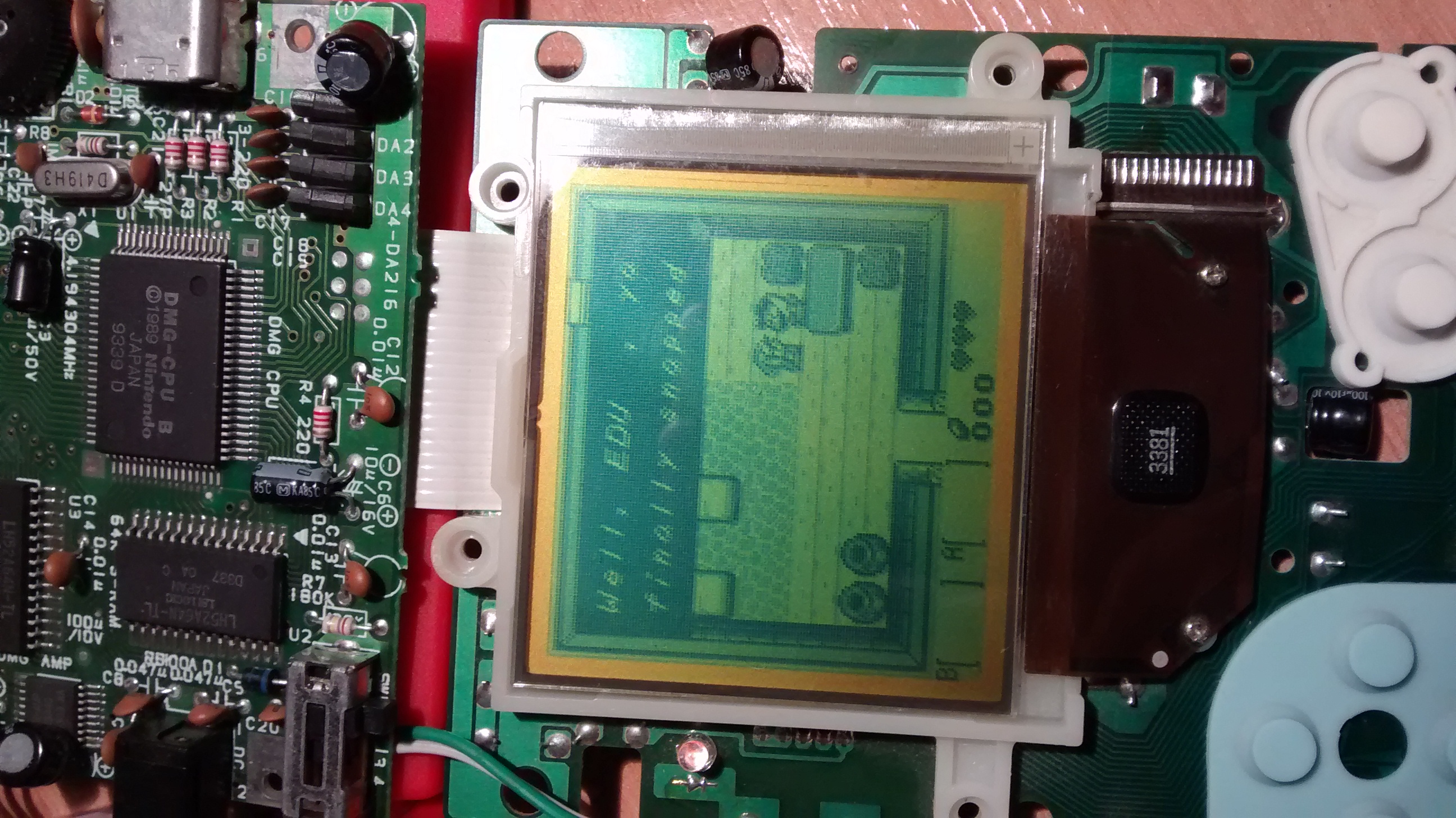
The Legend of Zelda. MBC1 game. Showing the cart RAM usage (The name, EDU, is saved in the cartridge RAM)

Dr. Mario. ROM Only game
Videos
Running The Legend of Zelda, - Link’s Awakening, showing that the cartridge RAM is working.
Running the demo 20y by Snorpung.
Conclusions
Being able to emulate a full cartridge with its RAM and memory banking with an ARM development board was really awesome. I wasn’t sure this was doable, and hadn’t seen anything similar. I don’t own any gameboy flashcarts, so being able to run code on the gameboy from something I built was extremely satisfactory. I enjoy watching works of demoscene, and with this project I was able to try out many amazing demos on the GameBoy.
On the technical side, this project took me a few days of fine tunning and adding capabilites. This was my first time developing on the STM32F4 so I also spent a few days documenting myself. The biggest issue I have found is the timing constraints. Adding cases to if statements, changin the order of some operations, modifying code… all this modifies the timing of the instructions generated by the compiler, sometimes not very intuitively due to strong compiler optimizations. I spent some hours of trial and error checking that all the operations worked fine. Also you may have noticed that all the code runs inside the interruption handler. And this handler is triggered at 1MHz! This gives a tight margin of operation. If the operations inside the interrupt takes too long, they will mask the next interruption and a following read/write operation (in case there was one) will be missed, probably crashing the GameBoy. Care must be taken to not exceed this timing constraint.
In the following post I will write about adding a custom boot logo to the cartridge emulator. Stay tunned!
Continuation: Booting the GameBoy with a custom logo