In these series of blog posts I will write about the Game Boy serial communication protocol and how to interact with it by using an embedded development board. The code for the development board will be written in C, and the code running on the computer will be written in Rust.
The first part will consist on understanding the Game Boy serial communication protocol, becoming familiar with embedded development using the libopencm3 free/libre library and finally building a serial communication sniffer to capture the transmission of data on the Game Link Cable.
The second part will focus on understanding the protocol used in the Game Boy printer, and how to build a virtual printer to store images on our computer (instead of actually printing them).
The third and final part will focus on printing on the Game Boy printer from our computer (without using a Game Boy).
Intro
In this post I will be explaining how I build a Game Boy serial communication sniffer using an ARM embedded development board. I will start by explaining how the Game Boy serial protocol works, then we will become familiar with the particular development board I will be using and the library to use its peripherals, and finally I will explain how I built the sniffer.
For this project I choose to use the NUCLEO-F411RE development board from STMicroelectronics, which is based on the STM32F411 ARM microcontroller, which runs at 100MHz, has many GPIOs, and has one USART conveniently connected to a USART to USB interface. One of the reasons to choose this board is it’s low price. Instead of using the official ST library for the microcontroller to manage its hardware I decided to try the libopencm3 library, a free/libre low level hardware library for many ARM Cortex-M3 and M4 microcontrollers.
The list of materials used in this project are the following:
- Game Boy Game Link Cable, $1.77 (at AliExpress)
- NUCLEO-F411RE, $13 (at Mouser, at Farnell)
- Dupont Wire Jumper cables with at least one Female tip, $1 (at AliExpress)
Game Boy serial protocol
The Game Boy (and the Game Boy Color) have a serial communication port that was used for two player games as well as to interface with peripherals like the Game Boy Printer. The serial protocol is quite simple. In the following drawing you can see what each of the 6 pins on the port do (from the cable point of view):
Game Link Cable connector pins
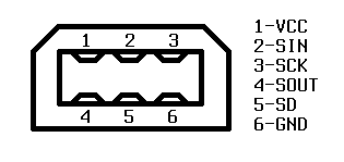
For a serial communication two devices will be connected together: a master and a slave. The master will control the clock (SCK) signal which indicates when bits start and stop. The master will be sending data to the slave through the Serial Out (SOUT) line while the slave will be sending data to the master through the Serial In (SIN) line. The SD line is not used in games nor the Game Boy Printer, and it’s not clear if it’s used in any way. All signals work at 5V TTL.
The original Game Boy dives the clock (SCK) at 8192 Hz, allowing a transfer rate of 1 KB/s.
Data is sent and received in bytes, and the master decides when a byte is both sent (SOUT) and received (SIN), which happens at the same time (basically, the two devices will exchange a byte).
This byte transfer can be easily implemented by having a byte register on every device which keeps shifting out a sending bit and shifting in a receiving bit on every clock cycle. The bit shifted out will be the most significant one and the bit shifted in will be the least significant one. After 8 clock cycles, the two devices will have exchanged a complete byte. The following diagram shows the byte register state at transfer each cycle (taken from the Pan Docs):
o7 o6 o5 o4 o3 o2 o1 o0
o6 o5 o4 o3 o2 o1 o0 i7
o5 o4 o3 o2 o1 o0 i7 i6
o4 o3 o2 o1 o0 i7 i6 i5
o3 o2 o1 o0 i7 i6 i5 i4
o2 o1 o0 i7 i6 i5 i4 i3
o1 o0 i7 i6 i5 i4 i3 i2
o0 i7 i6 i5 i4 i3 i2 i1
i7 i6 i5 i4 i3 i2 i1 i0
The following Oscilloscope capture of a serial communication shows the transfer of a few bytes. Since the bits are shifted out from the most significant bit of the transfer byte, the order of bits will be from 7 to 0:
, with overlay information added by me](../../media/gameboy_serial/Sigint_112_www.mikrocontroller.net_0_info.jpg)
Oscilloscope capture by Sigint 112 posted at www.microcontroller.net, with overlay information added by me
As we can see from the oscilloscope capture, the bit value is put on the data line when the clock signal falls and is replaced by the next bit at the next clock signal fall. This means that a good opportunity to read the bit value is when the clock signal rises.
Working with libopencm3 and the NUCLEO-F411RE
The NUCLEO-F411RE is an ARM development board based the STM32F411RET6 microcontroller (based itself on the ARM Cortex-M4). The CPU can run at 100 MHz and it has 512 KB of Flash and 128 KB of SRAM. The board has an ST-LINK/V2 which allows programming and debugging the microcontroller via USB as well as offering a virtual serial port (connected to one of the USARTs). You can learn about all the pins functionalities and the jumper configurations in the NUCLEO-64 datasheet. To program the board you will want to take a look at the datasheets of the STM32F411RET6 and its periferals.
As with the STM32F4-Discovery, most of the pins of the NUCLEO-F411RE are 5V tolerant, so connecting the GPIOs to the Game Boy serial port won’t be an issue.
This is the first project I’ve done using the libopencm3 library, and I have to say that I prefer it over the official ST one. Not only libopencm3 is fully free/libre software, I found it to be better documented. Nevertheless, the library documentation will not be sufficient to successfully use all the peripherals, you will need to read the STM32F411RET6 datasheets in order to understand how to configure them properly (that is, understand which GPIOs are can be routed to which peripherals, learn about the different DMA streams and channels, etc.).
For a good introduction to start using libopencm3 on the NUCLEO-F411RE, and to avoid feeling overwhelmed about all the datasheets, I recommend taking a look at the libopencm3-examples repository. First try the NUCLEO-F411RE examples which should work out of the box, and play a bit with them. You can also take a look at the STM32F4-Discovery examples, which are more complete. Try to adapt them to the NUCLEO by checking the datasheet for the proper configuration (you may even not need to change anything!).
The STM32 microcontroller can run at different frequencies, which can be configured in the code itself. Nevertheless, this configuration is not straightforward: the board includes a clock source and which is multiplied and divided by several configurable multipliers and divisors. This means that we can’t get any frequency we want. Moreover, the CPU frequency must be a multiple of the APB1 bus frequency. Not only that, but if I understood it correctly, the APB1 needs to be set at 48 MHz if we want the USB peripheral to be working correctly. libopencm3 has some default frequency configurations, but unfortunately the highest one we can use with the STM32F411 is 84 MHz. After learning about the frequencies configuration from Tilen Majerle’s website, I managed to find a setup to get 96 MHz (which is the closest I could get to the 100 MHz). Notice that by default the NUCLEO-F411RE is connected to an external 8 MHz oscillator, but an internal oscillator can also be selected through jumpers configuration.
Here’s a snippet of code showing the clock configuration at 96 MHz and enabling the peripherals we will be using.
/* STM32F411-Nucleo at 96 MHz */
const struct rcc_clock_scale rcc_hse_8mhz_3v3_96mhz = {
	.pllm = 8,
	.plln = 384,
	.pllp = 4,
	.pllq = 8,
	.pllr = 0,
	.hpre = RCC_CFGR_HPRE_DIV_NONE,
	.ppre1 = RCC_CFGR_PPRE_DIV_2,
	.ppre2 = RCC_CFGR_PPRE_DIV_NONE,
	.power_save = 1,
	.flash_config = FLASH_ACR_ICEN | FLASH_ACR_DCEN |
		FLASH_ACR_LATENCY_3WS,
	.ahb_frequency  = 96000000,
	.apb1_frequency = 48000000,
	.apb2_frequency = 96000000,
};

static void
clock_setup(void)
{
	rcc_clock_setup_hse_3v3(&rcc_hse_8mhz_3v3_96mhz);
	//rcc_clock_setup_hse_3v3(&rcc_hse_8mhz_3v3[RCC_CLOCK_3V3_84MHZ]);

	/* Enable GPIOA clock for LED & USARTs. */
	rcc_periph_clock_enable(RCC_GPIOA);

	/* Enable GPIOC for game link pins. */
	rcc_periph_clock_enable(RCC_GPIOC);

	/* Enable clocks for USART2. */
	rcc_periph_clock_enable(RCC_USART2);

	/* Enable DMA1 clock */
	//rcc_periph_clock_enable(RCC_DMA1);
}
Implementing a sniffer
Now that we have learned about the Game Boy serial communication protocol and how to work with the NUCLEO-F411RE we can proceed with the project: building a sniffer to view the data that is being transferred over the Game Link cable.
To be able to tap into the Game Link lines, I took a Game Link cable, cut it in half, soldered a jumper at each line, and then joined it back. I connected the lines as in the following table:
- SCK -> PA0
- SIN -> PC0
- SOUT -> PC1
- SD -> PC2
I found it convenient to use constants to define the GPIO port (GPIOP_XXX) and GPIO number (GPION_XXX) for each line:
#define GPIOP_SCK  GPIOA
#define GPION_SCK  GPIO0

#define GPIOP_SIN  GPIOC
#define GPION_SIN  GPIO0

#define GPIOP_SOUT GPIOC
#define GPION_SOUT GPIO1

#define GPIOP_SD   GPIOC
#define GPION_SD   GPIO2
The hardware setup looks like this:
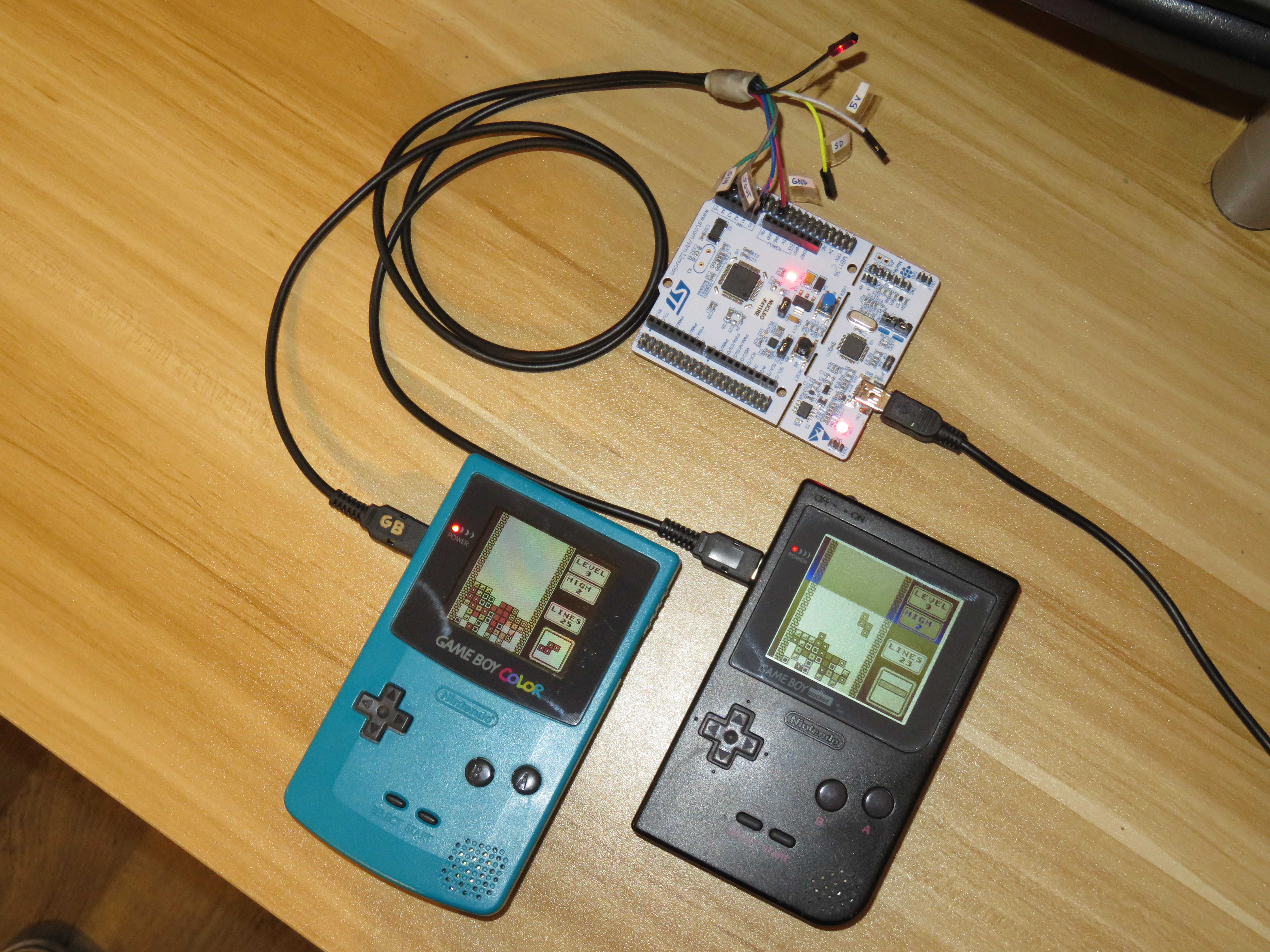
Sniffing setup with two player mode in Tetris
The way the sniffer will work is by reading the SIN and SOUT signals at every SCK cycle, building up the transferred bytes and sending them in pairs of (SOUT, SIN) over the USART that is connected to the ST-LINK which is connected via USB to my computer exposing a virtual serial device. On the computer side I will receive the data and present it nicely with a program written in Rust.
The following snippet will be required to setup the GPIO pins that are connected to the ST-LINK to work as USART (which is the alternate function number 7).
static void
gpio_setup(void)

	/* Setup GPIO pins for USART2 transmit. */
	gpio_mode_setup(GPIOP_USART, GPIO_MODE_AF, GPIO_PUPD_NONE, GPION_USART_TX | GPION_USART_RX);

	/* Setup USART2 TX/RX pin as alternate function. */
	gpio_set_af(GPIOP_USART, GPIO_AF7, GPION_USART_TX | GPION_USART_RX);
}
Then we configure all the GPIOs to which we have connected the Game Link Cable as input, and enable an external interrupt that will trigger when the logic level of the SCK signal rises (at which point we will read the SIN and SOUT signals).
static void
gblink_sniff_gpio_setup(void)
{
	// PA0 -> SCK
	gpio_mode_setup(GPIOP_SCK, GPIO_MODE_INPUT, GPIO_PUPD_NONE, GPION_SCK);
	// PC0 -> SIN
	gpio_mode_setup(GPIOP_SIN, GPIO_MODE_INPUT, GPIO_PUPD_NONE, GPION_SIN);
	// PC1 -> SOUT
	gpio_mode_setup(GPIOP_SOUT, GPIO_MODE_INPUT, GPIO_PUPD_NONE, GPION_SOUT);
	// PC2 -> SD
	gpio_mode_setup(GPIOP_SD, GPIO_MODE_INPUT, GPIO_PUPD_NONE, GPION_SD);

	nvic_set_priority(NVIC_EXTI0_IRQ, 0);
	nvic_enable_irq(NVIC_EXTI0_IRQ);

	exti_select_source(EXTI0, GPIOP_SCK);
	//exti_set_trigger(EXTI0, EXTI_TRIGGER_FALLING);
	exti_set_trigger(EXTI0, EXTI_TRIGGER_RISING);
	exti_enable_request(EXTI0);
}
libopencm3 uses fixed function names to handle interrupts. In our case we are using the external interrupt 0 that triggers when SCK goes low, so we define the function exti0_isr that will be called on that event. We store the values of SIN and SOUT in gb_sin and gb_sout and keep shifting them until we’ve received 8 values, at which point we have the entire SIN and SOUT byte that we send over USART.
volatile uint8_t gb_sin, gb_sout;
volatile uint8_t gb_bit;

void
exti0_isr(void)
{
	exti_reset_request(EXTI0);

	// RISING
	gb_sin |= gpio_get(GPIOP_SIN, GPION_SIN) ? 1 : 0;
	gb_sout |= gpio_get(GPIOP_SOUT, GPION_SOUT) ? 1 : 0;
	gb_bit++;

	if (gb_bit == 8) {
		// Send gb_sin and gb_sout over USART2
		usart_send_blocking(USART2, gb_sin);
		usart_send_blocking(USART2, gb_sout);

		// Reset state
		gb_bit = 0;
		gb_sin = 0;
		gb_sout = 0;
	} else {
		gb_sin <<= 1;
		gb_sout <<= 1;
	}
}
Finally, on the computer side, we read the serial data over USB by using the Rust serial port crate. Considering that in the Game Boy serial protocol, every time the master sends a byte it also requests a byte from the slave, which may have nothing to send, I expect that often transferred bytes will be just 0x00, so I decided to hide those values from the output to make it easy to focus on the important parts. The output format for every byte pair is {SOUT}:{SIN}.
fn mode_sniff<T: SerialPort>(port: &mut BufStream<T>) -> Result<(), io::Error> {
    let mut buf = vec![0, 0];
    loop {
        try!(port.read_exact(&mut buf));
        let sdout = buf[0];
        let sdin  = buf[1];
        let sdout_s = if sdout == 0 { format!("") } else { format!("{:02x}", sdout) };
        let sdin_s  = if sdin  == 0 { format!("") } else { format!("{:02x}",  sdin) };
        print!("{}:{} ", sdout_s, sdin_s);
        io::stdout().flush()?;
    }
}
As a bonus, here you can find the serial communication capture of playing Tetris in multiplayer mode. It would be easier to reverse engineer the protocol used in Tetris if you are able to experiment with the game yourself, but at first sight it doesn’t seem too complicated. For instance, during the playing part, each Game Boy sends to each other the height of their accumulated blocks using the lowest nibble of the transferred byte.
I’ve also made a capture of the data transferred to the Game Boy Printer by the Game Boy Camera to print a photo. We will use this capture in the next part of these posts to understand how the Game Boy Printer protocol works. And here’s a picture of the setup:

Sniffing setup with Game Boy Camera connected to the Game Boy Printer
To see the full source code of this project, check out the following repositories:
- gb-link-stm32f411: the code that runs on the NUCLEO-F411RE
- gb-link-host: the code that runs on the computer
The source code contains the three parts of the project joined into a single code base.
See you on the second part in which I’ll explain how I built a Game Boy virtual printer to send pictures taken from the Game Boy Camera to my PC by simulating a Game Boy Printer. Coming soon!