Introduction
The following project consists on emulating the functionality of a GameBoy cartridge with the development board STM32F4. The system is fully functional and is able to emulate real cartridges (as well as homebrew games) of the type ROM Only and MBC1 (Memory Block Controller 1). In this post I will explain how I managed to achieve this.
Motivation
Current flashcart systems commonly use a design consisting on a FPGA or CPLD controlling the logic of the emulated cartridge (memory banking, RAM access, etc.), a media storage (flash chip or SD card) and an SDRAM chip.
The way this flashcarts work is that upon booting the console, they present a small program that list the ROMs available in the media storage. The user selects a game and the FPGA copies it from the media storage to the SDRAM to allow fast access. Once the ROM has been copied, the FPGA acts as a gateway mapping the contents of the SDRAM to the original cartridge mappings.
Since the GameBoy cartridges use small ROM chips for which one can find compatible FLASH chips in the market, it is a viable alternative to the FPGA to take an original cartridge with a MBC5 and swap the original ROM chip with a compatible FLASH memory. A cartridge with MBC5 is often selected because with it, games with ROM Only and games using MBC1 can also be run (There is compatibility). With this setup, the user is able to reprogram the FLASH many times with different games and play them on the GameBoy.
This procedure is detailed here: DIY Nintendo GAMEBOY Classic Flash Cartridge
The FPGA system seems to allow much more freedom but it also involves more work: the MBC5 (or the supported Memory Block Controllers) must be implemented in hardware, an interface to access the media storage must be designed, the circuit must be designed too with all the components (FPGA/CPLD, FLASH/SD Reader, SDRAM, …).
An alternative to this one can think of would be to use a microcontroller instead, interfacing the cartridge pins through the GPIO. This design can have many complications since the timings to perform a read / write operation are quite tight. The microcontroller should be fast enough to perform this operations at the bus speed. When adding the functionality of the Memory Block controller the timings could be hard to achieve. Alex from Inside Gadgets attempted to achieve this using an Arduino. The low frequency of the Arduino made this project infeasible, although Alex was able to achive the emulation of the Nintendo logo, due to the fact that when the gameboy boots, the first read of the Nintendo logo from the cartridge is timming predictable and not too fast:
My aim was to try to implement a cartridge emulator using a faster microcontroller.
The hardware
For this project I choosed the STM32F4 Discovery. This development board features an ARM Cortex-M4 which can run at 168MHz, with 1 MB Flash, 192 KB RAM and more than 70 GPIO. The GPIO are accessed through a peripherials bus that can run at 100MHz. I also considered other boards such as the Teensy 3.1 but I ended up choosing the STM32F4 because it had more Flash and RAM and because it was unexpensive (14€).
On the other side, the GameBoy CPU runs at 4MHz. The comercial cartridges have up to 512 KB of ROM and 128 KB of RAM, although the MBC5 is capable of handling bigger ROMs. Many cartridges have a MBC (Memory Block Controler) such as the MBC5 or the MBC1. This controller allows the catridge to handle ROMs that don’t fit into the GameBoy memory area reserved for the cartridge ROM by means of bank selection. This selections are performed by writting into specific areas of the memory map reserved for the ROM (So that the MBC can handle them).
A list of characteristics of the comercial cartridges can be found here: GB Cart List It is important to notice that the GameBoy works at 5V whereas the STM32F4 works at 3.3V. Connecting 5V signals to the GPIOs of a 3.3 microcontroller can be dangerous and damage the GPIO peripherials. Luckily the STM32F4-Discovery has 5V tolerance for most of the pins. To see which ones you can check the documentation.
With these characteristics it seems this project can be doable. If we consider that the gameboy will perform at most a read / write per CPU cycle (We will later see that this is not the case), we are left with 42 cycles of our dev board to handle the operation. Taking into account that the GPIO bus is clocked at 100MHz, there will be some delay which will leave us fewer cycles.
Analyzing the bus
In order to get an idea of how the bus used by the GameBoy to access the cartridge works I decided to perform some captures using a Logic Analyzer. Since I don’t have any hardware logic analyzer, I used a an awesome project which consists of an implementation of a logic analyzer for the STM32F4, which uses the SUMP protocol to interface with the PC (SUMP is a standard protocol for hardware logic analyzers to interface with the client side). The logicdiscovery allows to sample up to 20MHz on 16 channels, with up to 24k samples:
The client used is the Logic Sniffer, an open source Java client compatible with the SUMP protocol:
In order to analyze the bus while the GameBoy was performing reads and writes to the cartridge, I soldered an FDD ribbon to the main board of the GameBoy, intercepting the cartridge pins as follows:
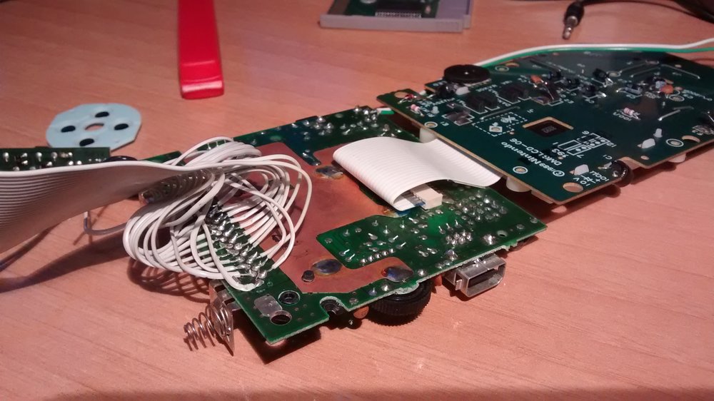
Back of the GameBoy PCB with the cartridge pins soldered to a FDD ribbon.
Since only 16 channels are available for the logicdiscovery I decided to monitor the CLK, RD, WR, CS, DATA {0-4} and ADDR {0-8}. (That is, the lower 4 bits of the data and the lower 8 bits of the address). With this we should be able to get information about the timings of the different operations.
The GameBoy cartridge pinout is well known, so it’s easy to figure out what every pin on the PCB of the GameBoy does from a pinout picture:
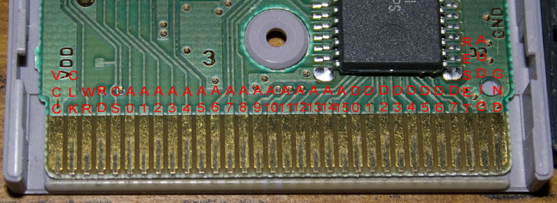
GameBoy cartridge pinout. Image from www.insidegadgets.com
Results
Upon analyzing the bus with the BATMAN game (ROM Only cartridge), the following is obtained:
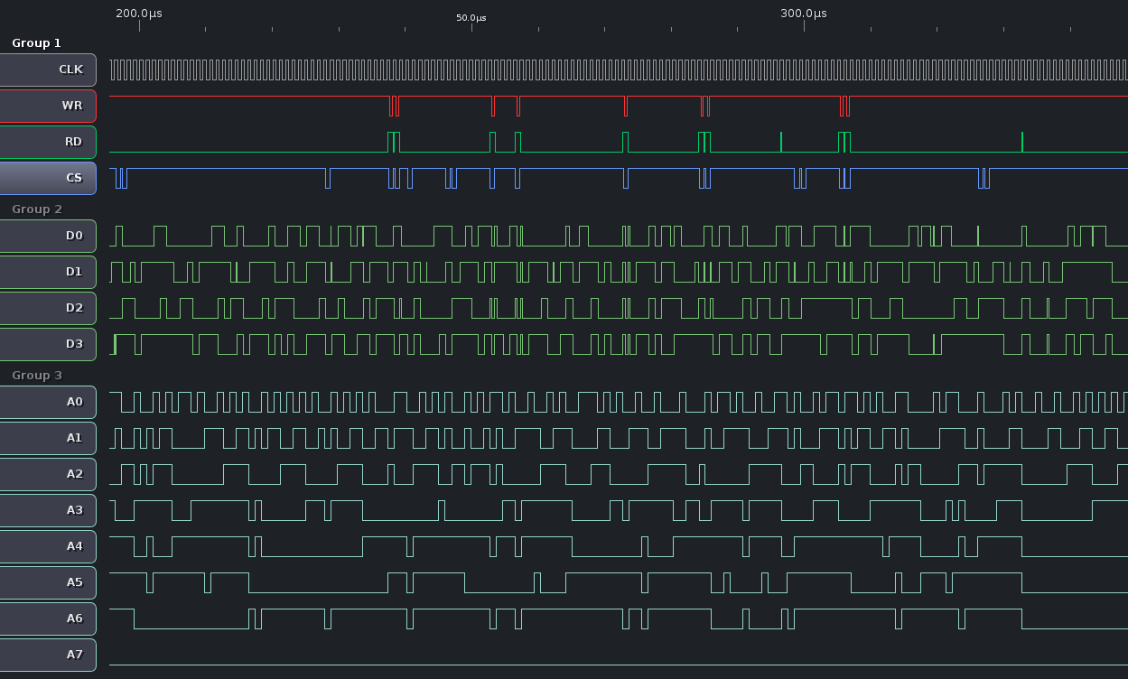
Logic capture overview
The first thing I noticed is that the CLK is at 1MHz, this is good news for us: we have more cycles for each operation. One oddity I found with the capture is that we can see that the WR goes low a few times (WR is active on low). The BATMAN cartridge doesn’t have RAM nor Memory Block Controller, so it doesn’t make sense to write into it. Since we only have half of the adressess, we can’t say for certain where the data is being written, but my guess is that we are seeing writes being done to the internal GameBoy RAM.
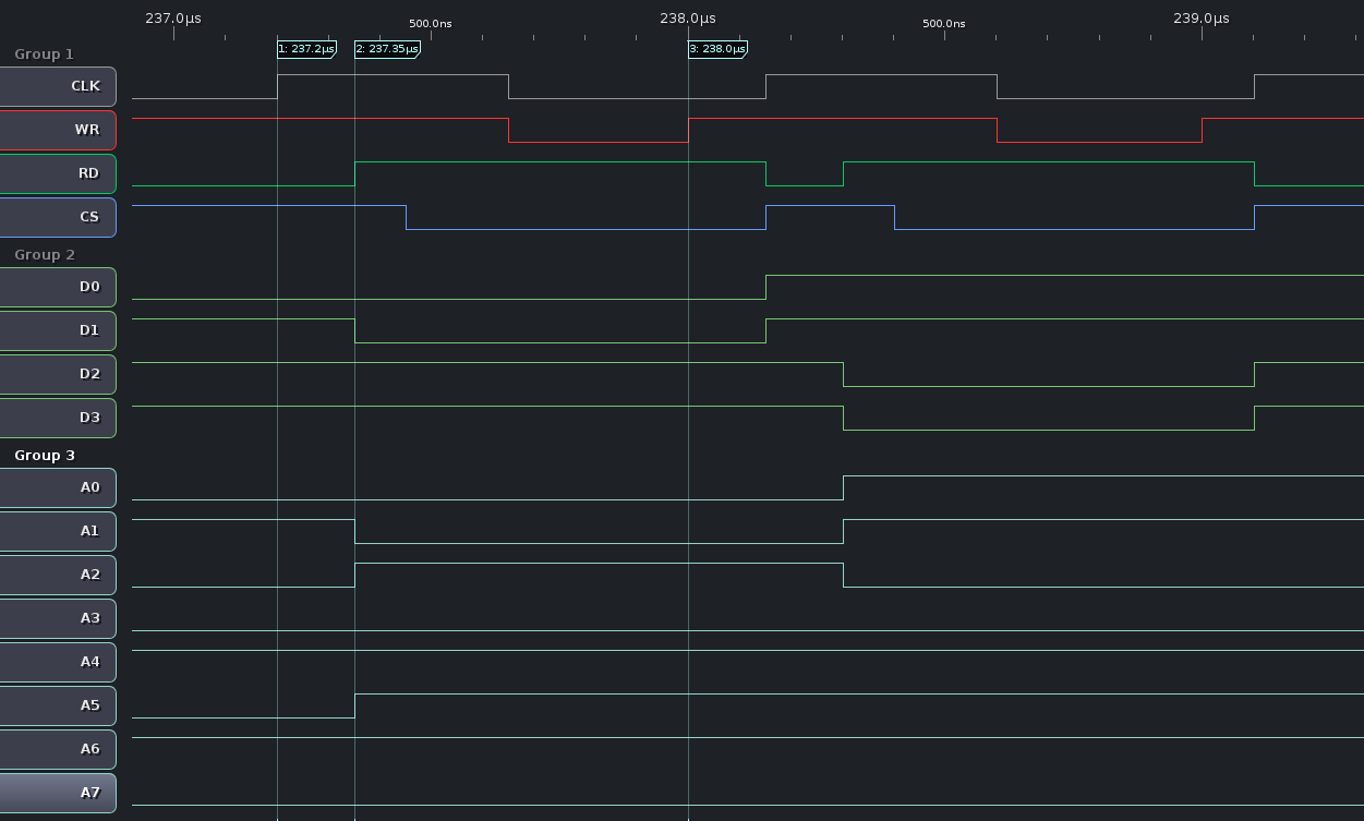
We can take a closer look to a read and a write and analyze what’s happening and when. This information will give us an idea on when should we perform the reading of the adresses for a write/read operation, and when to output the data on a read operation.
Notice that we have a 20MHz sampling rate, this means that a sample is being taken every 50 ns, leading to an error of +/- 25 ns.
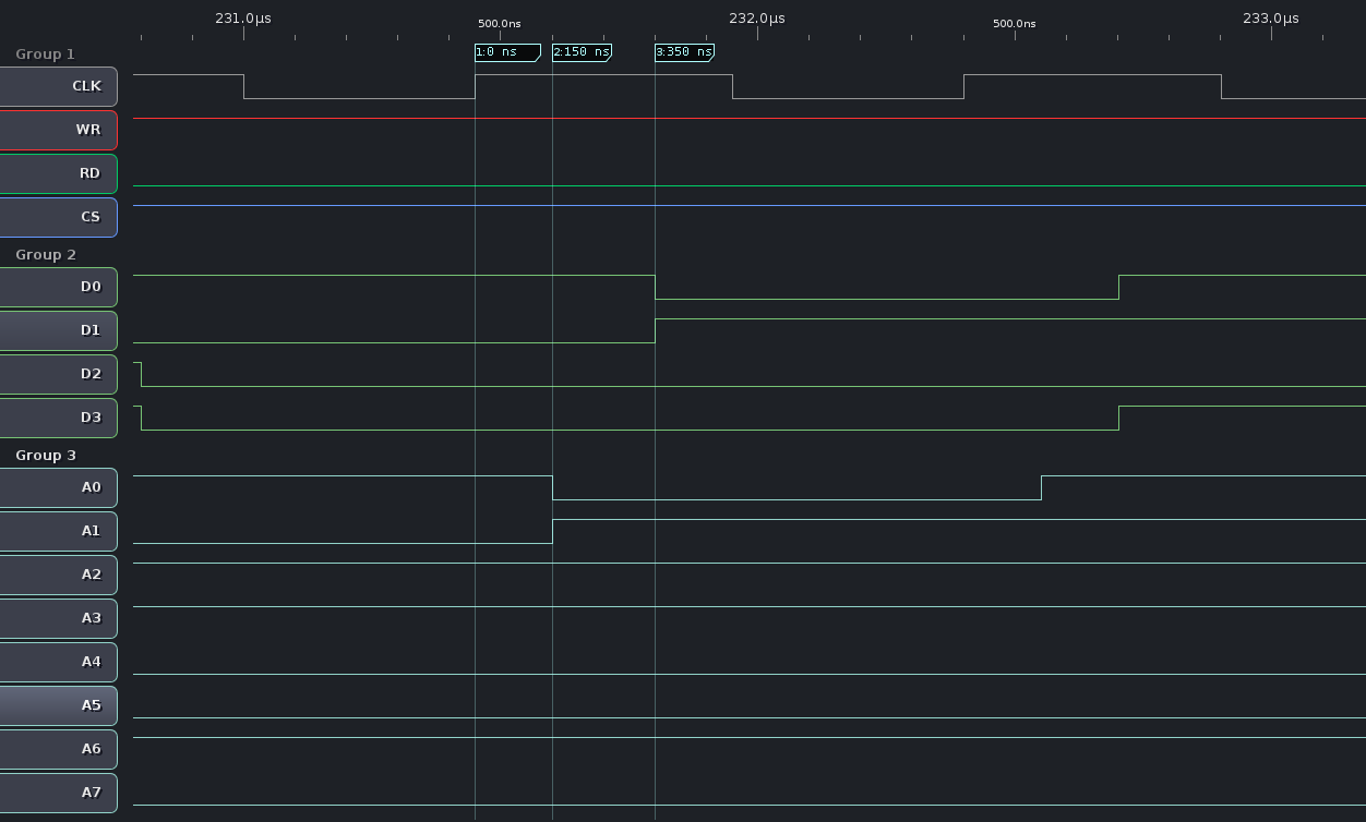
Read timings
Write timings
We can see that for a read operation, the GameBoy leaves WR and CS unactivate (high) and the RD active (low). This is the default. The GameBoy sets the address 150ns after the CLK rise, and the data is available in the bus (coming from the cartridge) 200 ns later. We can’t say when the GameBoy reads the data, but a guess would be around the CLK fall.
For the write operation, the RD is set to unactive at the same time the address and the data is set in the bus (150 ns after CLK rise). 100 ns later the CS is activated. At the CLK fall, the WR is activated, allowing the cartridge to perform the write for 300 ns. On the next cycle, we can see that RD and CS are reset to the default state (low and high, active and unactive respectively). Notice that the CS (Chip Select) is not strictly needed, although it seems to be used only when accessing RAM (this is not clear).
The writing timing analysis are sound with the analysis found in the unnoficial GameBoy CPU Manual:
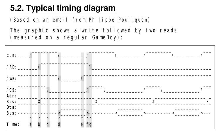
RAM timings, taken from the Game Boy CPU Manual. Click for detailed timings.
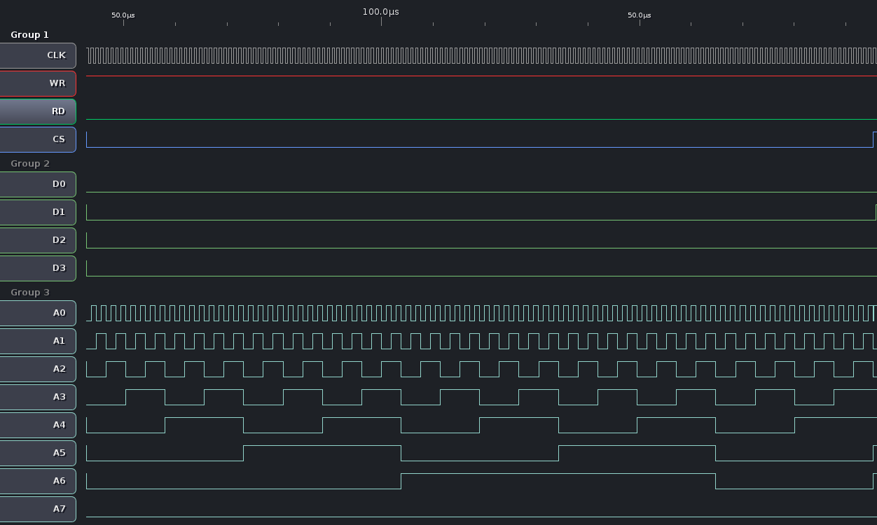
Now that we know that the information seen in the bus is not only the communication between the GameBoy and the cartridge but all the read/write operations of the GameBoy to its memory map, we can understand the following capture, which shows a DMA operation (The GameBoy has a DMA functionality to allow to fast copy contents from RAM or ROM to the OAM (Object Atribute Memory), used by the screen to draw sprites):
DMA in action
In the following post I will write about the implementation of the cartridge emulator. Stay tunned!
Continuation: Emulating a GameBoy Cartridge with an STM32F4. Part 2