Introduction
For the past few years I have been interested in the Game Boy: I’ve written an emulator in C (without sound), I developed a physical cartridge “emulator” using a microcontroller, and most recently I’ve built a project to interface my PC with the Game Link. I’ve also played a bit with Game Boy programming.
In the past I considered buying a Game Boy flashcart so that I could run demos and other scene ROMs on real hardware comfortably, but the price of such carts is a bit high. After some reading on reddit, I learned that Chinese manufacturers are selling unlicensed Game Boy cartridges at very cheap prices ($5). Not only that, but these cartridges use flash memory to store the ROM, and so have the potential to be reflashed! I confirmed this fact after learning about a commercial device called the jeoy-joebag, developed by BennVenn
With all this, I decided to build a Game Boy cartridge reader/writer.
On one hand, the device would allow reading the ROM and SRAM of the cartridge, supporting several memory block controllers (that’s the mechanism Game Boy cartridges use to access more memory than the supported by the 16 bit address space that the Game Boy offers). Also rewriting the SRAM would be straightforward. This is already an interesting project, as it allows dumping ROMs from physical cartridges, storing saves, and rewriting them (with the possibility of editing the saved game on your computer). I built a device that allows all this using the NUCLEO-F411RE ARM development board programmed using the libopencm3. I wrote the computer side software in Rust. Information about how to build such system is widely available on the Internet, so I will not be explaining how to do it. There are already several other projects that do this like the Arduino based GBCartRead by Alex from Inside Gadgets.
What I will be explaining is how to reflash a Game Boy Chinese cartridge, which I haven’t found explained anywhere. I’ll give details on how I figure out the process.
Information gathering
I started by ordering two Game Boy Chinese cartridges from AliExpress. I choose two games that have big ROMs, to make sure the corresponding flash chip in the cartridges would be big enough to fit most of the Game Boy ROMs. The games were:
        Game name           |          Cart type         | ROM (Kb) | RAM (Kb)
----------------------------|----------------------------|----------|---------
Grandia - Parallel Trippers | ROM + MBC5 + RAM + Battery |   4096   |   32
Dragon Warrior III          | ROM + MBC5 + RAM + Battery |   4096   |   32
My first idea was to take a look inside, figure out the flash chip model, find the datasheet and learn how such flash chip is reprogrammed. Here’s a picture of the cartridges:
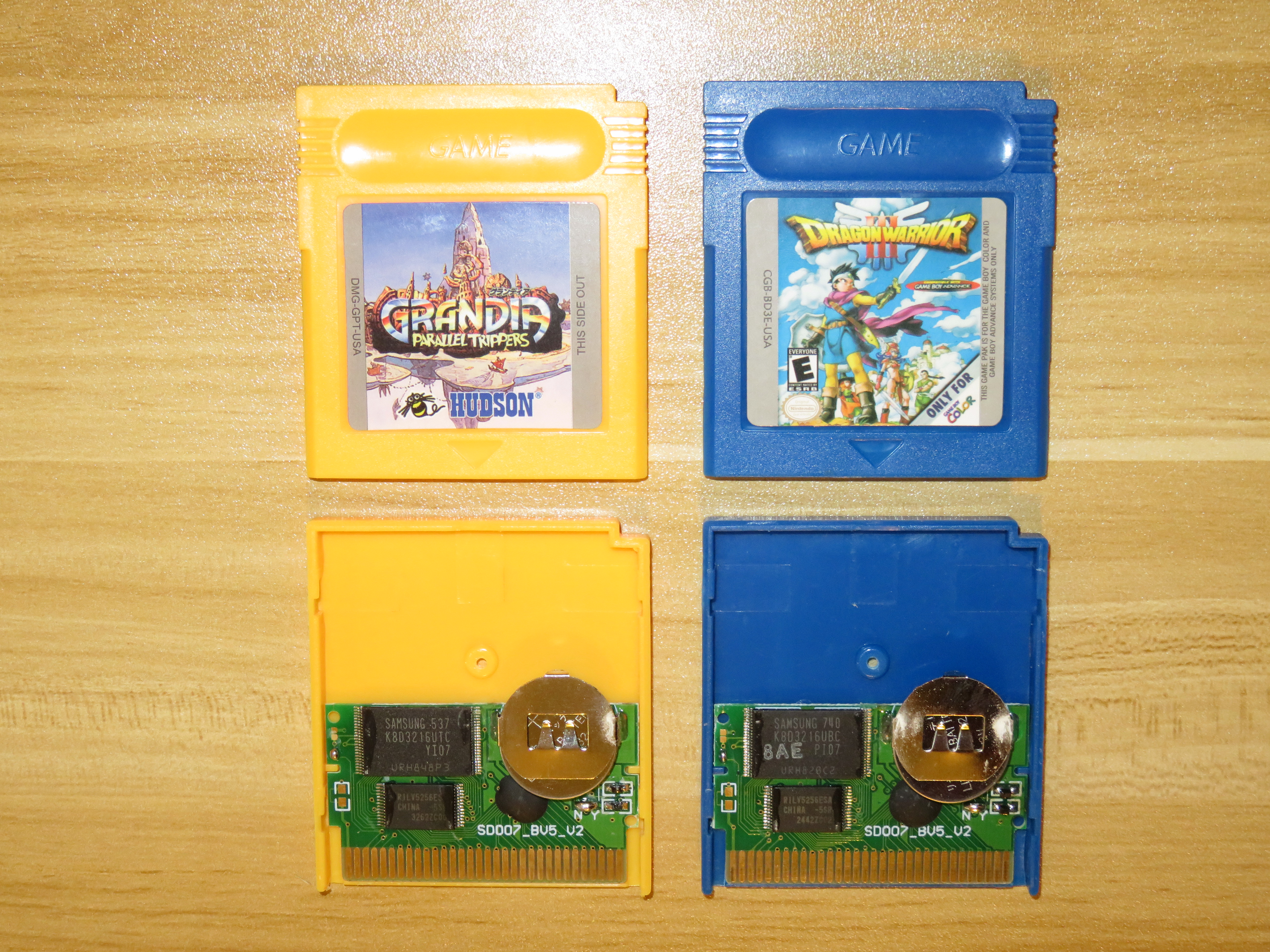
Inside of Game Boy Chinese cartridges.
We can see that each PCB has two chips that can be seen, a blob and a battery. Under the blob there’s probably a chip that acts as a memory controller (MBC5), then one chip will be the flash and the other the SRAM, which keeps its memory after the Game Boy powers off thanks to the battery. I couldn’t find any datasheet on any of the chips, the most I could find are references to the SAMSUNG chips, which seem to be the flash chips. How do we proceed from here?
I came up with two procedures to figure out how to flash the cartridges. The first one is preferable, mainly because the second one may end up being unsuccessful. Due to my circumstances, I had to follow the second one, and luckily I was successful.
Reverse engineering a patched Game Boy ROM from a Chinese cartridge without battery
I’ve learned that some of the Game Boy Chinese cartridges are sold without battery in them. Since the cartridge requires a battery to keep the data in the SRAM chip, what the Chinese manufacturers do is patch the ROM they write into the flash such that every time the game saves its state, it reflashes a part of the flash to store the contents of SRAM. That means that the Game Boy is running a code that flashes the cartridge from which its running.
What I would do if I had such a cartridge would be to dump it and run it through a Game Boy emulator (ideally one with debugging capabilities). Then I could cause the game to save its state and analyze what’s going on internally. Specifically, I would be monitoring reads to the cartridge ROM address space.
Another way to learn how things go would be to disassemble the dumped ROM and analyze the saving routines. To help with this I would first obtain the original ROM dump of the game and compare the disassembly of it with the Chinese patched ROM with a tool like diffoscope to learn in which routines were added (which would be the ones that program the flash memory).
Unfortunately I don’t own any Game Boy Chinese cartridge without battery, so I can’t proceed with this idea.
Figuring out the flashing procedure by looking at documentation of similar chips and experimenting
I would expect that even if there are different manufacturers producing flash chips, they would have a similar procedure for flashing. There’s no need for them to reinvent the wheel.
So I found a candidate chip with available datasheet, the MX29LV320AT/B, which is described as a “32M-BIT [4M x 8 / 2M x 16] SINGLE VOLTAGE 3V ONLY FLASH MEMORY”. The Game Boy Chinese cartridges also use flash chips at 3V despite the original cartridges working at 5V. Even though this MXIC flash chip is bigger than the Game Boy ROMs, I hope its interface is general enough that I can learn from it to figure out how to program the flash in the Chinese cart.
And so we search the datasheet for the documentation on how to program the chip:
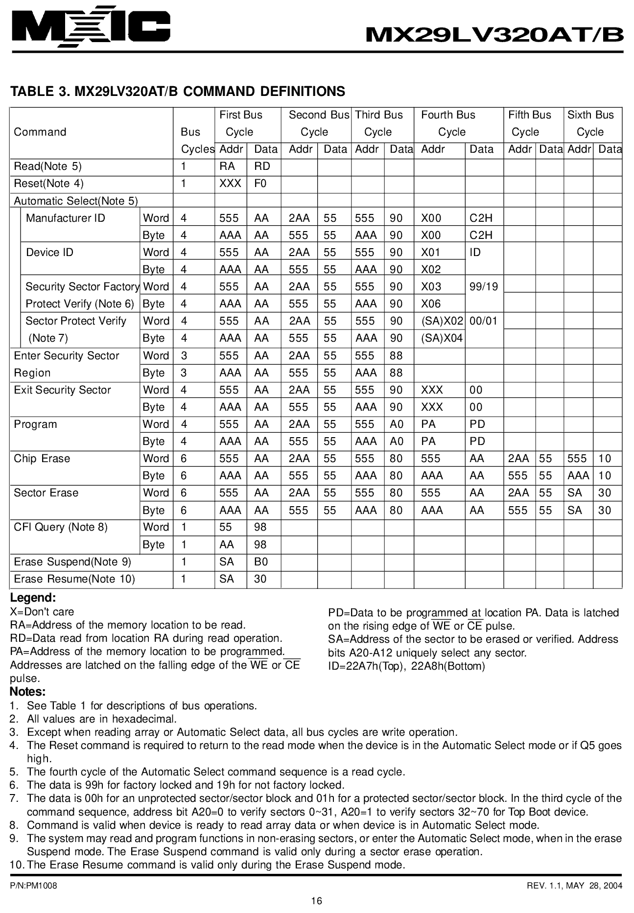
Screen capture of MX29LV320AT/B flash memory datasheet showing available commands.
We can see that all the commands start with the same pattern, by performing writes using constant addresses and data values. By doing a web search using the terms “0xAAA 0xAA flash” we can see several results that seem to indicate that these commands could be common for flash chips. For example, take a look at this source code.
Great, now we have some lead to follow for an experiment.
Figuring out the flash commands
Using the MXIC chip documentation we can start with a first experiment: Let’s try the commands in the datasheet, if they work we may already be able to program the chip. Considering that the Game Boy cartridge data bus is 8 bit, I will be trying the “byte” commands.
So the first experiment will consist of running the “Manufacturer ID” command. This command is performed by 3 writes followed by one read, which will return the Manufacturer ID instead of the data in the read address. We can easily test if this command is working by reading the value at the 0x000 address and comparing it to the Manufacturer ID that is returned after performing the 3 writes followed by a read at 0x000. If the values differ it means that the command is working.
Unfortunately the value we read after running the command is not different than the value at address 0x000, so the command is not working.
Here are some hypothesis of what’s going on:
- The commands for our flash chip are completely different than the ones in the datasheet we are looking at
- Every manufacturer has a slight difference in the constant values used in the commands.
- The manufacturer of the flash chip found in the Chinese cartridge has modified some of the constant values in the commands as a form of obfuscation to deter users from reprogramming the flash chip.
I’m inclined to believe that the third hypothesis is what’s actually happening, as I have found many references of the flash commands found in the MXIC datasheet for several other manufacturer’s chips.
Let’s build an experiment based on the hypothesis that data values (0xAA and 0x55) used in the commands are considered two magic numbers, and the manufacturer has decided to use different ones. Luckily the space of these magic numbers is 16 bit, so we can brute force them to verify the hypothesis.
I wrote a code to try all the combinations of the magic numbers for the NUCLEO-F411RE, which has a Game Boy cartridge slot connected via GPIOs. The C code is pretty straight forward: It will read the value at 0x000, send it over USART, and then run the command to get the Manufacturer ID in a loop trying all possible values for the magic numbers. Once the right magic numbers are found (that’s when the value returned by the command is different than the value found at 0x000), the values are sent over USART.
uint8_t magic0, magic1, cmd, v0, v;
uint16_t a0, a1, a2, a3;
uint8_t buf[12];

a0 = 0x0AAA;
a1 = 0x0555;
a2 = 0x0AAA;
a3 = 0x0000;

cmd = 0x90;

// Reset
bus_write_byte(0x0000, 0xF0);

v0 = bus_read_byte(a3);
buf[0] = a3 & 0xFF; buf[1] = a3 >> 8;
buf[2] = v0;
usart_send_bytes_blocking(buf, 3);

buf[0] = a0 & 0xFF; buf[1] = a0 >> 8;
buf[3] = a1 & 0xFF; buf[4] = a1 >> 8;
buf[6] = a2 & 0xFF; buf[7] = a2 >> 8;
buf[9] = a3 & 0xFF; buf[10] = a3 >> 8;

magic0 = 0x00;
magic1 = 0x00;
do {
        do {
                bus_write_byte(a0, magic0);
                buf[2] = magic0;
                bus_write_byte(a1, magic1);
                buf[5] = magic1;
                bus_write_byte(a2, cmd);
                buf[8] = cmd;
                v = bus_read_byte(a3); // Manufacturer ID
                buf[11] = v;
                if (v != v0) {
                        usart_send_bytes_blocking(buf, 12);
                        goto end;
                }
                gpio_toggle(GPIOP_LED, GPION_LED);
        } while (magic1++ != 0xFF);
} while (magic0++ != 0xFF);
end:
I wrote a simple python script to receive the data the NUCLEO-F411RE is sending and format it nicely before printing it:
import serial, sys

with serial.Serial('/dev/ttyACM0', 1000000) as ser:

    data = ser.read(3)
    a3 = data[0] + (data[1] << 8)
    v0 = data[2]
    print('                         R: {:03X}:{:02X}'.format(a3, v0))

    while True:
        data = ser.read(3)
        a0 = data[0] + (data[1] << 8)
        magic0 = data[2]

        data = ser.read(3)
        a1 = data[0] + (data[1] << 8)
        magic1 = data[2]

        data = ser.read(3)
        a2 = data[0] + (data[1] << 8)
        cmd = data[2]

        data = ser.read(3)
        a3 = data[0] + (data[1] << 8)
        v = data[2]

        print('W: {:03X}:{:02X} {:03X}:{:02X} {:03X}:{:02X}, R: {:03X}:{:02X}'.format(a0, magic0, a1, magic1, a2, cmd, a3, v))
        if v != v0:
            print('MAGIC0: {:02X}, MAGIC1: {:02X}'.format(magic0, magic1))
            sys.exit(0)
The verdict
If the hypothesis is wrong, no combination of magic numbers will work and the value read at the end of the command will never return the Manufacturer ID. Thankfully the hypothesis seems to be right :) After a few short seconds of running the experiment, a pair of magic numbers is found that works:
                         R: 000:C3
W: AAA:A9 555:56 AAA:90, R: 000:EC
MAGIC0: A9, MAGIC1: 56
So we just need to replace the 0xAA and 0x55 from the commands in the datasheet by 0xA9 and 0x56 respectively.
Reprogramming the flash
One thing to be aware of when dealing with flash memories is that before writing anything you need to erase the sector. The flash memory is divided into sectors, and for writing, each bit in each sector can only turn from 1 to 0, and not the other way around. So to write arbitrary data, the first required step is erasing the sector, which will leave all the bits at 1, and then the program command can write any data by turning the appropriate bits to 0. Since I will be programing the entire flash every time, I will use a command that erases all sectors at once. Erasing the entire flash takes about a minute.
The code running on the NUCLEO-F411RE will run a loop waiting for commands from the PC, which are stored in a queue and executed in order. Some commands will put the microcontroller at a special state to receive data. I decided to use the queue approach (with the added complexity) instead of running the commands serially in a loop to achieve faster cartridge reading and writing speeds by using concurrency. In particular, for programming I use the DMA controller to receive the next ROM bank via USART to be programmed while at the same time the previous received ROM bank is being flashed. Similarly, for reading cartridges, while a read ROM bank is being sent over USART, the next bank is being read from the cartridge concurrently.
This helps accelerate the process because reading and specially writing the flash cartridge is slow (remember that the Game Boy works at 4 MHz, while the NUCLEO-F411RE works at 96 MHz). In a serial approach, while reading/writing the flash chip, the microcontroller would not be able to do anything else.
Finally, here’s a picture of my setup for the reader/writer. I soldered jumpers to a Game Boy Color cartridge slot I bought on AliExpress, and then connected it to the NUCLEO-F411RE GPIOs.
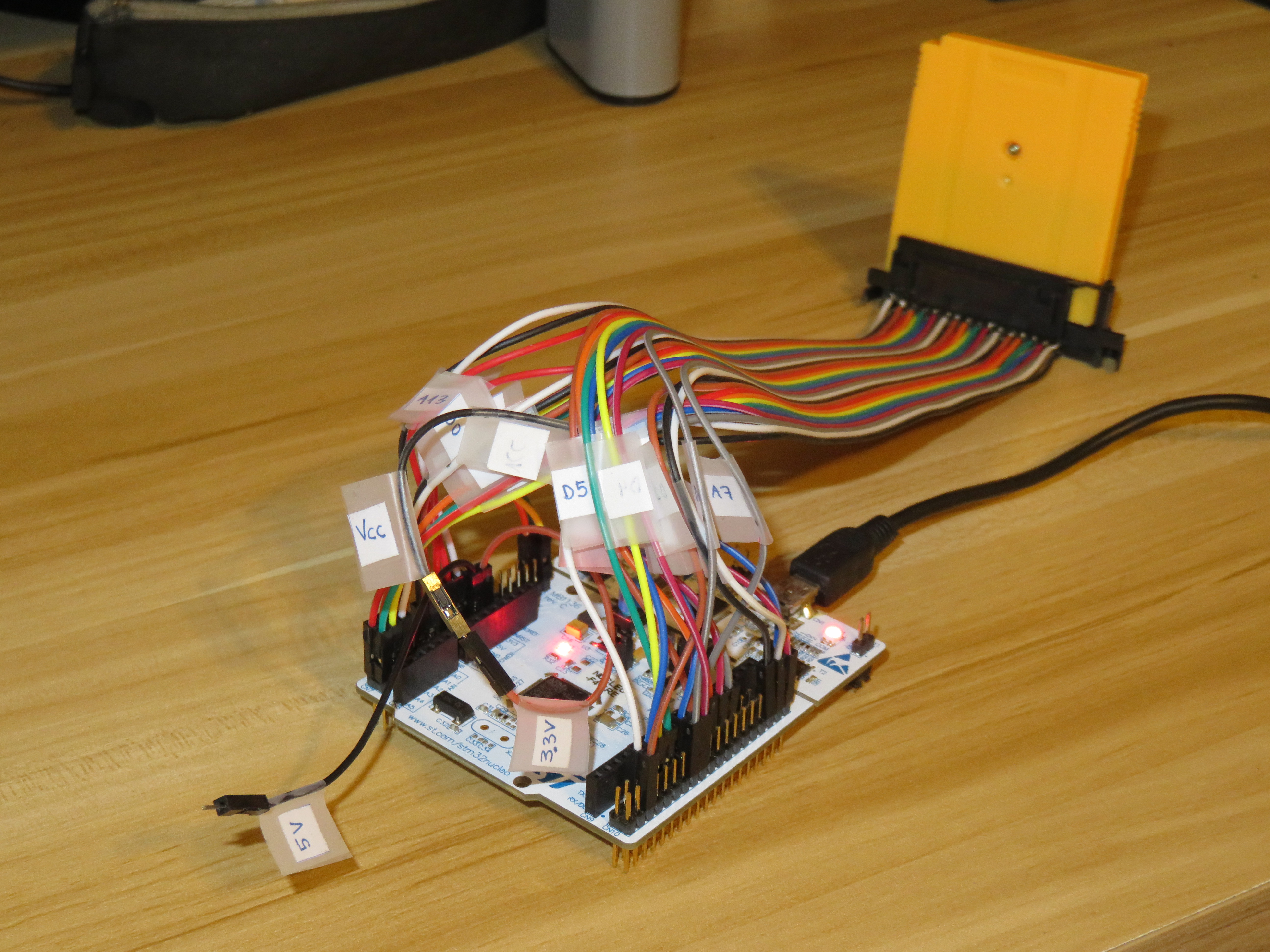
Setup with the NUCLEO-F411RE wired to a Game Boy cartridge connector.
You can find the full source code of this project on the following repositories:
- gb-rw-stm32f411: the code that runs on the NUCLEO-F411RE
- gb-rw-host: the code that runs on the computer
Some final notes on the NUCLEO-F411RE
DMA
A note on the DMA controller of STM32 microcontrollers: While DMA is transferring from USART to RAM and vice versa, the CPU can’t access RAM. This led me to think for some time that my approach was not increasing the speed of the process in any manner, while clearly adding lots of complexity. But after a second thought, and considering that the memory bus of the STM32 works using a round-robin schedule, I’m convinced there’s a speed improvement because the USART speed is much slower than the STM32 memory bus. This means that the DMA will be accessing the memory bus in batches, transferring chunks of data; and between these batches the CPU will be reading the code from RAM to execute it.
USART and DMA
Getting DMA to work (in my case, with USART) took some reading of datasheets. Reading the documentation of libopencm3 is not enough, as you need to know which DMA channel and stream to use for USART. Take a look at my code to see how it works!
NUCLEO-F411RE available pins
Originally I wanted to connect all the cartridge address pins to the GPIO C bus, which conveniently has 16 pins available on the board. I couldn’t get the system working: I kept getting random garbage when reading the cartridges. After reviewing all the code, all the connections and the soldering points, I found out the problem. Even though the GPIO pin PC14 and PC15 are exposed on the board, in most common setups they are connected to the external oscillator, so they can’t be used as GPIO pins! If you use them as input pins, you’ll just keep reading the oscillator values.